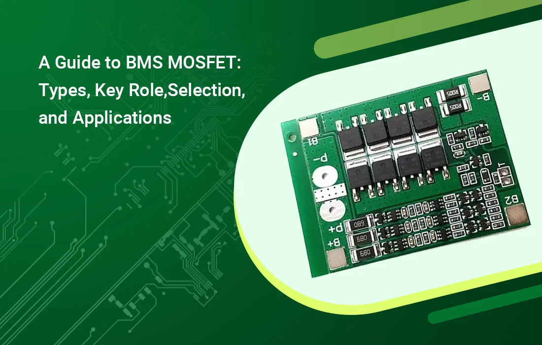
In our previous article, we introduced the BMS hardware and its key components, one of which is the MOSFET. The main function of lithium BMS is to realize intelligent management and maintenance of battery cells and to supervise the battery states through condition monitoring and abnormal fault protection. Among them, BMS MOSFETs play a big role in the protection of lithium battery boards, and the main role of MOSFETs is to detect overcharging, overcurrent during charging and discharging, and overcurrent during short-circuit. Therefore MOS products are widely used in BMS. This blog will mainly talk about the world of BMS MOSFET, and their types, purpose, advantages, applications, and how to choose.
What is a MOSFET?
A MOSFET (Metal Oxide Semiconductor Field Effect Transistor) consists of a MOS (Metal Oxide Semiconductor) structure combined with an FET (Field Effect Transistor). Applying a voltage to the metal gate and the source across the oxide insulating layer generates an electric field effect to control the semiconductor (S) conductive channel, allowing the MOSFET to function as a field effect transistor. Due to the isolation between the gate and source, and the gate and drain by the SiO2 insulating layer, the MOSFET is also known as an insulated gate field effect transistor.
Power field effect transistors on the market are usually referred to as insulated gate MOS or power MOSFETs. FETs are divided into two different structures: junction and insulated gate types. A FET is a semiconductor device that uses the electric field effect of the input circuit to control the output circuit current. It relies solely on the majority of carriers in the semiconductor to conduct electricity and is also known as a unipolar transistor.
The junction-type power FET is generally referred to as a static induction transistor (SIT). It is characterized by the gate voltage controlling the drain current, having a simple drive circuit, requiring a small drive power, fast switching speed, high operating frequency, and better thermal stability than the GTR. However, it has a small current capacity and low withstand voltage, generally only applicable to power electronic devices not exceeding 10kW.
MOSFETs, on the other hand, are primarily used as switches and drivers, operating in the switching state. They can withstand voltages ranging from tens of volts to thousands of volts, and the operating current can range from a few amperes to tens of amperes. Power MOSFETs are enhanced MOSFETs, which have excellent switching characteristics.
Types of BMS MOSFET
MOSFET consists of three terminals: the source, drain, and gate. According to the type of conducting channel, MOSFET can be divided into P-channel and N-channel. If based on the gate voltage amplitude, it can be divided into two modes: Depletion mode and Enhancement mode. When the gate voltage is zero there is a conducting channel between the drain and the source. For N (P) channel devices, the conducting channel exists when the gate voltage is greater than (less than) zero. Power MOSFETs are mainly N-channel enhancement types. According to the mentioned above, MOSFET can be classified as follows:
- P-Channel Enhancement
- P-Channel Depletion
- N-Channel Enhancement
- N-Channel Depletion
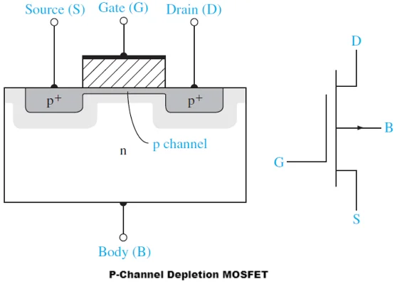
P-Channel MOSFET
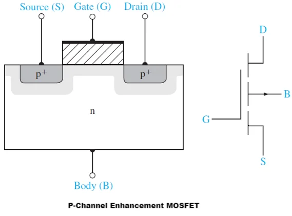
In a p-channel MOSFET, the source is connected to a positive voltage, and the FET conducts when the voltage on the top terminal falls below a certain broad value (Vgs 0). This means that if you want to use a P-channel MOSFET to switch voltages above 5V, you need another transistor (of some type) to turn it on and off.
The P-channel region is located between the source and drain terminals of a P-channel MOSFET. It is a four-terminal device with the following terminals: gate, drain, source, and body. The drain and source are p+ regions and the body or substrate is n-type. Current flows in the direction of positively charged holes.
When a negative voltage with repulsion is applied to the gate terminals, the electrons below the oxide layer are pushed downward into the substrate. The depletion region is filled with bound positive charges associated with the donor atoms. The negative gate voltage also attracts holes from the p+ source and drain regions into the channel region.
The p-channel depletion MOSFET is structurally the exact opposite of the n-channel depletion MOSFET. In this case, the pre-built channel is made of p-type impurities sandwiched between the heavily doped p-type source and drain regions. When we apply a positive voltage to the gate terminals, the electrostatic action attracts minority carriers, i.e., free electrons from the p-type region, resulting in the formation of static negative impurity ions. As a result, depletion regions are formed in the channel and the conductivity of the channel is reduced. We can control the drain current by applying a positive voltage to the gate.
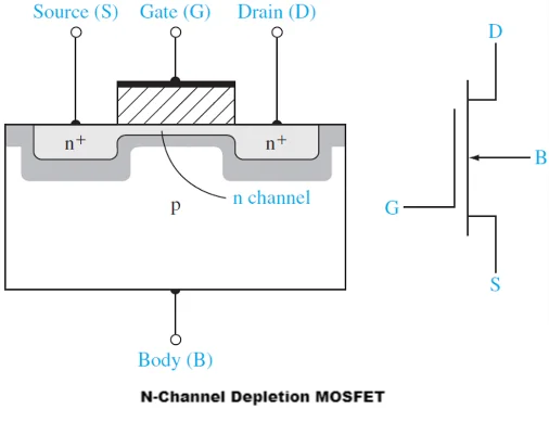
N-Channel MOSFET
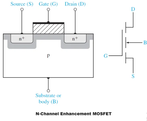
An N-channel MOSFET has its source grounded and its drain connected to the load, and the FET conducts when a positive voltage is applied to the gate. N-channel MOSFETs are the most common and easiest to use. They are also less expensive to produce and therefore less expensive and have higher performance than p-channel MOSFETs.
The N-channel region is located between the source and drain terminals. The drain and source terminals of this type of field effect transistor are heavily doped n+ regions, while the substrate or body is P-type. The current in this type of MOSFET is caused by negatively charged electrons. When a positive voltage with repulsive force is applied to the gate terminals, holes below the oxide layer are pushed downward into the substrate. Bound negative charges associated with the acceptor atoms fill the depletion region.
When the electrons reach the channel, the channel is formed. The positive voltage also draws electrons from the n+ source and drains regions into the channel. When a voltage is applied between the drain and source, current flows freely between them and the gate voltage controls the electrons in the channel. If we apply a negative voltage instead of a positive voltage, a hole channel is formed below the oxide layer.
N-channel MOSFETs work on the assumption that most carriers are electrons. The movement of electrons in the channel is responsible for the flow of current in the transistor. The formation of the gate terminals requires the use of p-substrate material.
The Purpose and Role of MOSFET in BMS:
In a BMS, battery MOSFETs serve as intelligent switches, enabling precise control over the charge and discharge processes of individual battery cells. Here are some of the key functions performed by MOSFETs in a BMS:
- Cell Balancing: MOSFETs facilitate the controlled discharge of higher-charged cells, ensuring that all cells within the battery pack are balanced and operating at optimal levels.
- Overcurrent and Short-Circuit Protection: By rapidly switching off the current flow, MOSFETs protect battery cells from potentially damaging overcurrent and short-circuit conditions.
- Thermal Management: MOSFETs can be used to disconnect cells or modules that exceed safe temperature thresholds, preventing thermal runaway and preserving the integrity of the battery pack.
Advantages of Using MOSFETs in BMS:
Incorporating MOSFETs in a BMS design offers several compelling advantages:
- Low On-Resistance: MOSFETs exhibit low on-resistance, minimizing power losses and improving overall system efficiency.
- High Switching Speed: With their fast switching capabilities, MOSFETs can respond quickly to changes in load conditions or fault scenarios, ensuring prompt protection and control.
- Compact Size: The small footprint of MOSFETs allows for space-efficient designs, making them ideal for compact battery management systems.
- Cost-Effectiveness: Compared to other switching devices, MOSFETs are generally more cost-effective, contributing to reduced overall system costs.
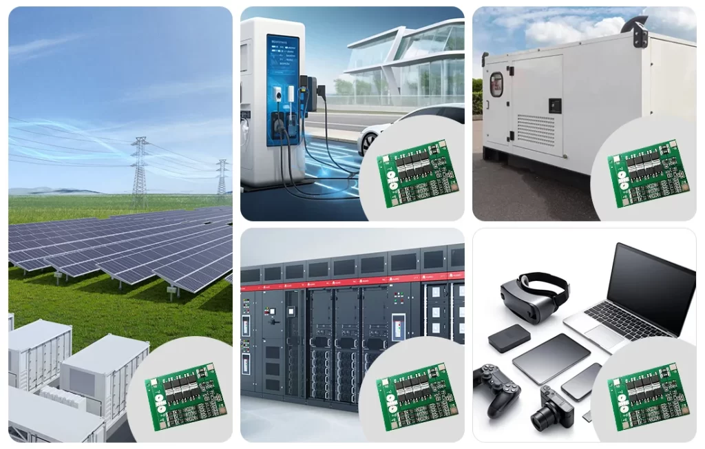
Applications of BMS MOSFETs:
The versatility and reliability of MOSFETs in BMS applications have made them indispensable in various industries:
- Electric Vehicles (EVs) and Hybrid Electric Vehicles (HEVs): Ensuring safe and efficient operation of high-voltage battery packs in electric and hybrid vehicles.
- Renewable Energy Systems: Enabling effective energy storage and management in solar, wind, and other renewable energy installations.
- Uninterruptible Power Supplies (UPS) and Backup Power Systems: Providing reliable power backup and protection for critical infrastructure and equipment.
- Portable Electronic Devices: Enhancing battery life and safeguarding lithium-ion batteries in laptops, smartphones, and other portable devices.
BMS MOSFET Selection
Choosing the appropriate MOSFET for a BMS application requires careful consideration of several key factors:
| Key Factors | Considerations |
| Voltage Rating | Withstand maximum voltage, including overvoltage conditions |
| Current Rating | Exceed the maximum expected current for safe operation |
| On-Resistance (RDS(on)) | Lower RDS(on) for reduced power losses and improved efficiency |
| Gate Charge | Impacts switching speed and power consumption |
| Thermal Management | Proper heat dissipation and package type selection |
- Voltage Rating: The MOSFET must be able to withstand the maximum voltage present in the battery pack, including any potential overvoltage conditions.
- Current Rating: Select a MOSFET with a current rating that exceeds the maximum expected current in the system, ensuring safe and reliable operation.
- On-Resistance (RDS(on)): Lower on-resistance translates to reduced power losses and improved efficiency. Choose a MOSFET with an appropriate RDS(on) for your application.
- Gate Charge: The gate charge determines the amount of energy required to switch the MOSFET on and off, impacting switching speed and power consumption.
- Thermal Management: Proper heat dissipation is crucial for MOSFETs, as excessive temperatures can degrade performance and reliability. Consider factors like package type and heatsinking requirements.
Conclusion
By understanding the purpose, advantages, and applications of BMS MOSFETs, as well as the key factors to consider during selection, engineers and designers can make informed choices that optimize system performance and longevity.
MOKOEnergy‘s commitment to excellence and its in-depth knowledge of MOSFET selection and implementation processes make it a trusted partner for organizations seeking cutting-edge BMS solutions. Whether you’re working on electric vehicles, renewable energy systems, or portable electronics, MOKOEnergy’s expertise can help you achieve your goals while ensuring uncompromising quality and reliability.
So, if you’re looking to unlock the full potential of your battery-powered systems, consider partnering with MOKOEnergy and benefit from their deep understanding of BMS MOSFETs and their unwavering dedication to customer satisfaction.